- 您现在的位置:买卖IC网 > Sheet目录2001 > ISL267817IUZ (Intersil)IC INTERFACE
ISL267817
6
FN7877.2
April 19, 2012
tdDO
DCLOCK Falling Edge to Next DOUT Valid
35
150
ns
tDIS
CS/SHDN Rising Edge to DOUT Disable Time
See Note 10
40
50
ns
tEN
DCLOCK Falling Edge to DOUT Enabled
22
100
ns
tf
DCLOCK Fall Time
1
100
ns
tr
DCLOCK Rise Time
1
100
ns
NOTE:
10. During characterization, tDIS is measured from the release point with a 10pF load (see Figure 4) and the equivalent timing using the ADS7817 loading
(3k, 100pF) is calculated.
Timing Specifications Limits established by characterization and are not production tested. +VCC = 5V, fDCLOCK =3.2MHz, fS = 200kSPS,
VREF =2.5V; VCM = VREF. Boldface limits apply over the operating temperature range, -40°C to +85°C. (Continued)
SYMBOL
PARAMETER
TEST CONDITIONS
MIN
(Note 6)
TYP
MAX
(Note 6)
UNITS
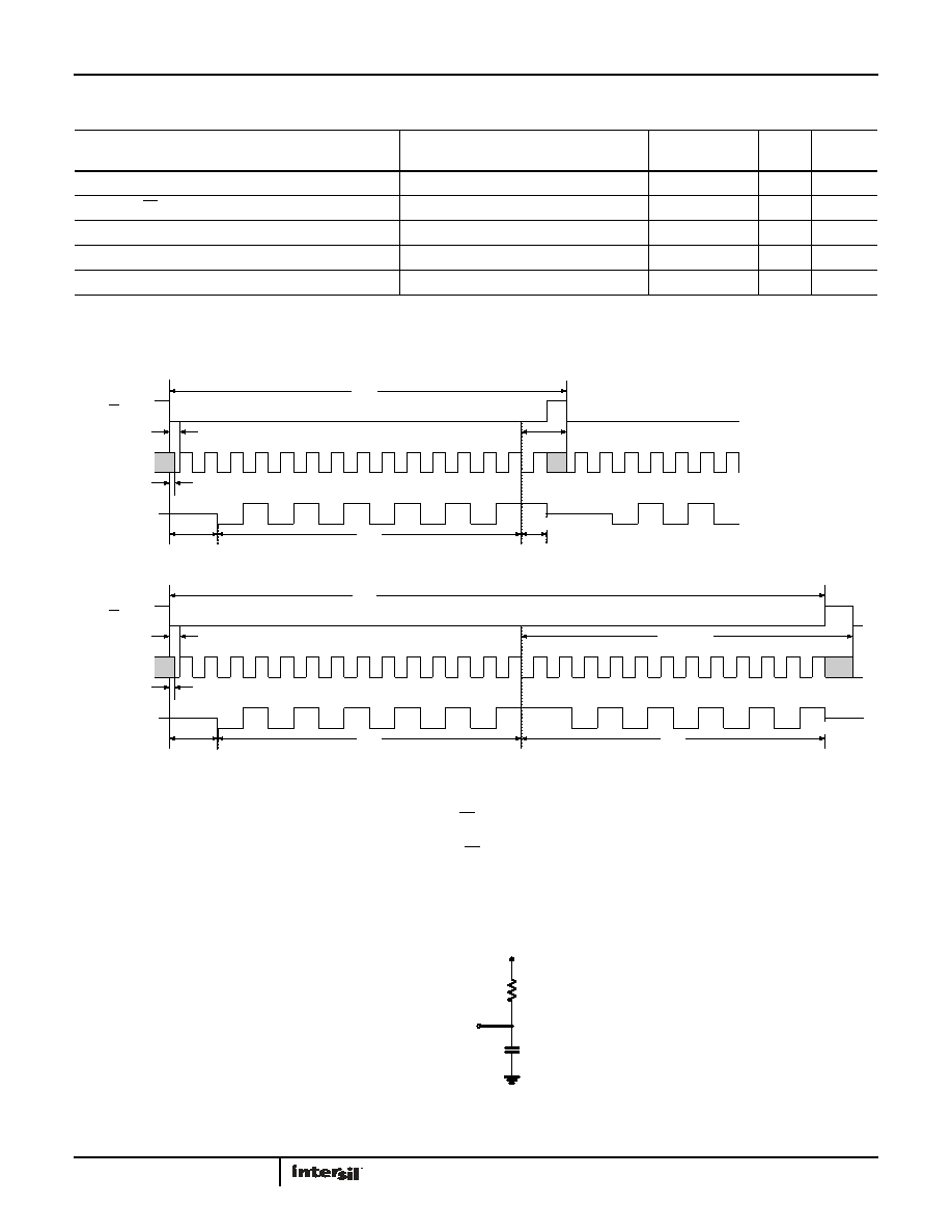
FIGURE 3. SERIAL INTERFACE TIMING DIAGRAM
NOTES:
11. After completing the data transfer, additional clocks applied while CS/SHDN is low will result in the previous data being retransmitted LSB-first,
followed by indefinite transmission of zeros.
12. After completing the data transfer, additional clocks applied while CS/SHDN is low will result in indefinite transmission of zeros.
tSUCS
B10
B9
B8
B7
B6B5B4B3B2
B1
B0
B11
B10
B9B8
NULL
BIT
Hi-Z
NULL
BIT
CS/SHDN
DCLOCK
DOUT
tCSD
tCYC
POWER
DOWN
tSMPL
tCONV
tDATA
tSUCS
B10
B9B8B7B6
B5
B4
B3
B2B1B0
B11
B10
B9
B8
NULL
BIT
Hi-Z
CS/SHDN
DCLOCK
DOUT
tCSD
tCYC
POWER
DOWN
tSMPL
tCONV
tDATA
B1
B2
B3
B4
B5
B7
B6
B11
(MSB)
B11
(MSB)
Note 12
Note 11
FIGURE 4. EQUIVALENT LOAD CIRCUIT
OUTPUT
PIN
CL
10pF
+VCC
2.85k
RL
发布紧急采购,3分钟左右您将得到回复。
相关PDF资料
ISL32272EIVZ-T
IC TX RS422 QUAD 16TSSOP
ISL32273EIVZ
IC RCVR RS485/422 QD ESD 16TSSOP
ISL32470EIBZ-T7A
IC TXRX RS485 FAULT PROT 14SOIC
ISL32483EIBZ-T7A
IC TXRX RS485 FAULT PROT 14SOIC
ISL35822LPIK
IC CLOCK/DATA RECOVERY 192EBGA-B
ISL41334IRZ-T7A
IC TXRX RS232/485 DL 2PRT 40QFN
ISL43485IB-T
IC TXRX 1TX/1RX 3V RS-485 8-SOIC
ISL51002CQZ-110
IC FRONT END 10BIT VID 128-MQFP
相关代理商/技术参数
ISL267817IUZ-T
功能描述:模数转换器 - ADC 12 BIT 200KSPS SAR 8LD 3 X 3 PROPRIETRY RoHS:否 制造商:Texas Instruments 通道数量:2 结构:Sigma-Delta 转换速率:125 SPs to 8 KSPs 分辨率:24 bit 输入类型:Differential 信噪比:107 dB 接口类型:SPI 工作电源电压:1.7 V to 3.6 V, 2.7 V to 5.25 V 最大工作温度:+ 85 C 安装风格:SMD/SMT 封装 / 箱体:VQFN-32
ISL267817IUZ-T7A
功能描述:模数转换器 - ADC 12 Bit 200kSPS SAR ADC 8LD RoHS:否 制造商:Texas Instruments 通道数量:2 结构:Sigma-Delta 转换速率:125 SPs to 8 KSPs 分辨率:24 bit 输入类型:Differential 信噪比:107 dB 接口类型:SPI 工作电源电压:1.7 V to 3.6 V, 2.7 V to 5.25 V 最大工作温度:+ 85 C 安装风格:SMD/SMT 封装 / 箱体:VQFN-32
ISL28005
制造商:INTERSIL 制造商全称:Intersil Corporation 功能描述:Micropower, Rail-to-Rail Input Current Sense Amplifier with Voltage Output
ISL28005_10
制造商:INTERSIL 制造商全称:Intersil Corporation 功能描述:Micropower, Rail-to-Rail Input Current Sense Amplifier with Voltage Output
ISL28005_11
制造商:INTERSIL 制造商全称:Intersil Corporation 功能描述:Micropower, Rail-to-Rail Input Current Sense Amplifier
ISL28005FH-100EVAL1Z
功能描述:数据转换 IC 开发工具 ISL28005FH EVALRD 1 5LD GAIN OF 100
RoHS:否 制造商:Texas Instruments 产品:Demonstration Kits 类型:ADC 工具用于评估:ADS130E08 接口类型:SPI 工作电源电压:- 6 V to + 6 V
ISL28005FH100Z-T7
功能描述:电流灵敏放大器 ISL28005FH100Z MICRO PWR CUR SENSE AMP RoHS:否 制造商:Texas Instruments 通道数量: 共模抑制比(最小值):110 dB 输入补偿电压:80 uV 电源电压-最大:5.5 V 电源电压-最小:2.7 V 电源电流:350 uA 最大工作温度:+ 125 C 最小工作温度:- 40 C 安装风格:SMD/SMT 封装 / 箱体:VQFN-16 封装:Reel
ISL28005FH100Z-T7A
功能描述:电流灵敏放大器 ISL28005FH100Z MICRO PWR CUR SENSE AMP RoHS:否 制造商:Texas Instruments 通道数量: 共模抑制比(最小值):110 dB 输入补偿电压:80 uV 电源电压-最大:5.5 V 电源电压-最小:2.7 V 电源电流:350 uA 最大工作温度:+ 125 C 最小工作温度:- 40 C 安装风格:SMD/SMT 封装 / 箱体:VQFN-16 封装:Reel